DC2391A
Demonstration Board, LTC5589IUF#PBF, 700MHz to 6GHz, Low Power Direct Quadrature Modulator


Need more?
| Quantity | Price (Incl GST) |
|---|---|
| 1+ | $261.050 ($300.2075) |
Product Information
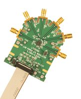
Product Overview
DC2391A demonstration circuit 2391A is optimized for evaluation of the LTC®5589 low power I/Q modulator up to 4.5GHz. For frequencies above 4.5GHz, LO matching circuit on the DC2391A demo board can be easily modified for improved image rejection performance. The four balanced I- and Q-baseband input ports can be either AC-coupled with internal bias supplied, or DC-coupled from a source with a common-mode voltage level of about +1.4V. The SPI interface is used to set internal registers which control the gain, optimum centre frequency, I-offset, Q-offset and sideband suppression. In addition to the digital gain control with 1dB steps, there is an analogue gain control, VCTRL. An on-chip thermometer can be used to compensate for the gain vs temperature variations using a digital gain control change. The update can either be automatically triggered, or entirely switched off.
- 3.8V supply voltage
- Operating temperature range from -40°C to 105°C
Notes
ADI products are only authorized (and sold) for use by the customer and are not to be resold or otherwise passed on to any third party
Technical Specifications
Analog Devices
RF / IF
Demo Board LTC5589IUF#PBF
No SVHC (21-Jan-2025)
LTC5589IUF#PBF
Quadrature Modulator
-
Technical Docs (1)
Legislation and Environmental
Country in which last significant manufacturing process was carried outCountry of Origin:Philippines
Country in which last significant manufacturing process was carried out
RoHS
RoHS
Product Compliance Certificate