Print Page
NVMFD5C680NLT1G
Dual MOSFET, N Channel, 60 V, 60 V, 26 A, 26 A, 0.023 ohm

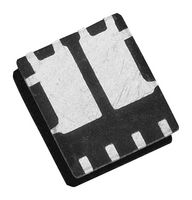
Image is for illustrative purposes only. Please refer to product description.
1,252 total stock globally
Need more?
1252 Delivery in 3-5 Business Days(UK stock)
| Quantity | Price (Incl GST) |
|---|---|
| 1+ | $3.280 ($3.772) |
| 10+ | $2.240 ($2.576) |
| 100+ | $1.610 ($1.8515) |
| 500+ | $1.460 ($1.679) |
Price for:Each (Supplied on Cut Tape)
Minimum: 1
Multiple: 1
$3.28 ($3.77 inc GST)
Line Note
Added to your Order Confirmation, Invoice, and Dispatch note for this order only.
This number will be added to the Order Confirmation, Invoice, Dispatch note, Web confirmation Email and Product Label.
Product Information
ManufacturerONSEMI
Manufacturer Part NoNVMFD5C680NLT1G
Order Code2835612
Technical Datasheet
Channel TypeN Channel
Drain Source Voltage Vds N Channel60V
Drain Source Voltage Vds P Channel60V
Continuous Drain Current Id N Channel26A
Continuous Drain Current Id P Channel26A
Drain Source On State Resistance N Channel0.023ohm
Drain Source On State Resistance P Channel0.023ohm
Transistor Case StyleDFN
No. of Pins8Pins
Power Dissipation N Channel19W
Power Dissipation P Channel19W
Operating Temperature Max175°C
Product Range-
Qualification-
SVHCLead (27-Jun-2024)
Product Overview
NVMFD5C680NLT1G is a dual N-channel power MOSFET. It has low RDS(on) to minimize conduction losses and low QG and capacitance to minimize driver losses.
- AEC-Q101 qualified and PPAP capable
- Drain-to-source breakdown voltage is 60V minimum at (VGS = 0V, ID = 250µA)
- Gate-to-source leakage current is 100nA maximum at (VDS = 0V, VGS = 20V)
- Negative threshold temperature coefficient is -4.3mV/°C typical at (TJ = 25°C)
- Drain-to-source on resistance is 23mohm typical at (VGS = 10V, ID = 5A)
- Input capacitance is 350pF typical at (VGS = 0V, f = 1MHz, VDS = 25V)
- Gate-to-drain charge is 0.8nC typical at (VGS = 4.5V, VDS = 48V; ID = 10A)
- Turn-on delay time is 6.4ns typical at (VGS = 4.5V, VDS = 48V, ID = 10A, RG = 1ohm)
- Rise time is 25ns typical at (VGS = 4.5V, VDS = 48V, ID = 10A, RG = 1ohm)
- Junction temperature range from -55°C to +175°C, DFN8 package
Technical Specifications
Channel Type
N Channel
Drain Source Voltage Vds P Channel
60V
Continuous Drain Current Id P Channel
26A
Drain Source On State Resistance P Channel
0.023ohm
No. of Pins
8Pins
Power Dissipation P Channel
19W
Product Range
-
MSL
MSL 1 - Unlimited
Drain Source Voltage Vds N Channel
60V
Continuous Drain Current Id N Channel
26A
Drain Source On State Resistance N Channel
0.023ohm
Transistor Case Style
DFN
Power Dissipation N Channel
19W
Operating Temperature Max
175°C
Qualification
-
SVHC
Lead (27-Jun-2024)
Technical Docs (2)
Legislation and Environmental
Country of Origin:
Country in which last significant manufacturing process was carried outCountry of Origin:Malaysia
Country in which last significant manufacturing process was carried out
Country in which last significant manufacturing process was carried outCountry of Origin:Malaysia
Country in which last significant manufacturing process was carried out
Tariff No:85412900
US ECCN:EAR99
EU ECCN:NLR
RoHS Compliant:Y-Ex
RoHS
RoHS Phthalates Compliant:Yes
RoHS
SVHC:Lead (27-Jun-2024)
Download Product Compliance Certificate
Product Compliance Certificate
Weight (kg):.000012